Experiential Learning | Research & Innovation | Community Impact | Career Preparation | Teaching Excellence | 21st Century Liberal Arts | Building Community | Good Vibes | CAS Spotlights | All Stories | Past Issues

Tiny Invisible Universes
DECEMBER 2, 2024
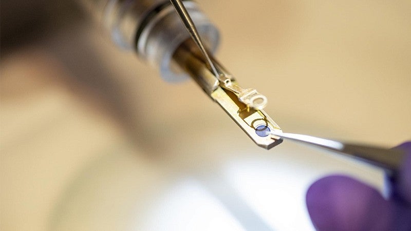
The world looks different in the laboratories buried 17 feet beneath campus, where you can pick up an object 1,000 times smaller than the width of a human hair and peer at its individual atoms.
Here, a Dorito looks like an alien landscape speckled with stalagmites of salt and fat. A human hair looks like a tree trunk. And a feather?
“Feathers look crazy. They’re disgusting, as it turns out,” says Valerie Brogden, nanofabrication and imaging facility director for the Center for Advanced Materials Characterization in Oregon (CAMCOR).
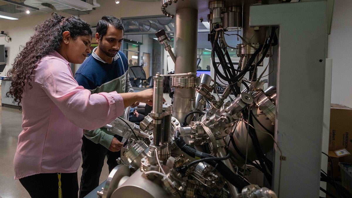
Equipped with some of the most powerful electron microscopes on the West Coast, CAMCOR is arguably the University of Oregon’s most comprehensive and cutting-edge core science facility. Funded by the Office of Research and Innovation, it was the first institute in North America to install a multi-ion source plasma focused ion beam, which can analyze and mill materials at the nanometer level, as well as the first user facility on the West Coast to house an image corrected transmission election microscope (TEM).
For years, CAMCOR has offered some of the best imaging resolution on the West Coast.
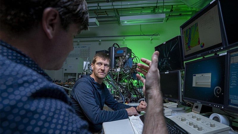
“We’re helping to advance science, to really push what can be done,” says CAMCOR facility director Kurt Langworthy. “We’re reinvesting in tools so we can resolve smaller features, improve chemical signals to understand composition at really minute length scales, and really understand a material’s properties at their very basics.”

Partnering with the semiconductor industry
Although its primary mission is to serve UO faculty and students, CAMCOR also provides materials characterization services to businesses—most notably those in the semiconductor industry.
Semiconductors, a key building block for electronic devices, are used in a wide range of products, from smartphones to cars.
“Our tools live in failure analysis labs at semiconductor companies,” Brogden says. “Semiconductor failure analysis is where our tools really shine.”
When a semiconductor device fails, it could mean there’s a miniscule defect within a single group of atoms. Discovering the source of the defect can require shaving off a cross-section of the diminutive device using a focused beam of ions—something Brogden routinely does in her lab—and examining it under an electron microscope.
“When you’re designing new semiconductor devices, there’s a bit of trial and error,” says high-resolution analytical facility director Josh Razink. “You process something, and it’s not as thick as you want it to be or doesn’t have as much purity as you want it to, so you ask, ‘Can we fix it or not? Is this a path worth continuing on?’”
As the demand for electronic goods continues to grow, the semiconductor workforce is expected to expand by nearly 115,000 jobs by 2030. The University of Oregon is a national leader in recruiting and training students for jobs in the semiconductor industry, and CAMCOR plays a key role in this initiative by teaching courses and hosting a master’s program that serves students interested in working at semiconductor companies.
“A lot of our students in the Advanced Materials Analysis and Characterization Master’s Program go on to work for the semiconductor industry,” Brogden says. “I would say the vast majority of them, because our tool sets are so very applicable to that industry.”
With CAMCOR’s focused ion beam scanning electron microscope (FIB-SEM), “we can look at things on the order of 10s of nanometers,” she says. (That’s about the size of a virus, which ranges in length from 30 to 50 nanometers.)

—Valerie Brogden, nanofabrication and imaging facility director for CAMCOR
Seeing the world through a transmission electron microscope
The microscopes at CAMCOR have opened a window for studying everything from semiconductor chips to human remains.
“A crime lab once brought a head in a box to us—like, a legit head in a box,” Langworthy recalls. “And they said, ‘Can you extract any metals from these rear molars? We believe a blade passed through this guy.’ And they peeled open this box and showed me the severed head with the molars fragmented.”
While Langworthy was able to find and analyze metal from the molars, his discovery didn’t yield any conclusive results, such as a suspect or murder weapon. But the experience underscores the range of possibilities offered in a place like CAMCOR.
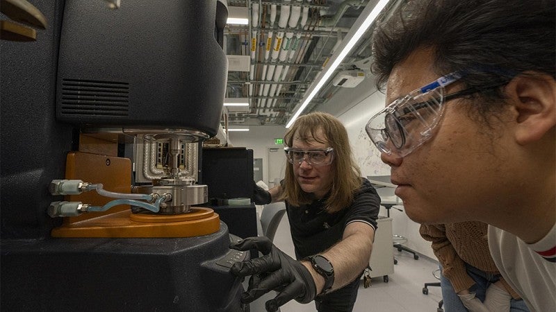
The shared facility is more than just a place where researchers can learn everything they want to know about a particular material, from its surface characteristics to its chemical composition. It’s also a place where students can gain valuable experience working with high-powered microscopes and other instruments used in the semiconductor industry, battery industry, biomedical and biotech, and aerospace companies such as SpaceX.

—Josh Razink, high-resolution analytical facility director for CAMCOR
Unlike a regular microscope, which passes light through an object, a transmission electron microscope sends an electron beam through it, allowing researchers to examine a material atom by atom, Razink says.
As semiconductor devices become smaller and smaller, CAMCOR will continue to seek new ways to improve its imaging capabilities, Langworthy adds.
"If we can surpass the resolution barrier of instrumentation, now you’re going to enable a lot of science to happen at length scales that used to be unimaginable.”
—By Nicole Krueger, College of Arts and Sciences
